Low Energy Electron Diffraction & Auger Electron Spectroscopy Data
Crystal Substrates > Si (110) - Silicon
Substrate Specifications
- Material: Silicon
- Size: 10 mm x 10 mm x 0.5 mm
- Orientation: (110)
- Structure: Cubic
- Lattice Constant: a= 5.43 Å
- Type/Dopant: N type, P doped
- Growth Method: Czochralski Method
- Melting Temperature: 1414 °C
- Debye Temperature (at 27 °C): 370 °C [Ref. 29]
- Surface Debye Temperature: Unpublished
- Characterization Tool: LEED-AES
Model: BDL800IR
- UHV Treatment: Annealing
- Applications: Solid state devices, microelectronics, laser, and in solar panels
LEED Patterns
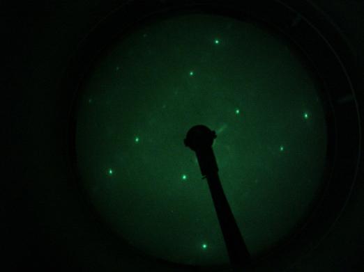 Si (110) - LEED Pattern 70 eV
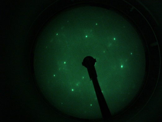 Si (110) - LEED Pattern 90 eV
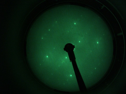 Si (110) - LEED Pattern 130 eV
Related Links