ocivm.com > Science & Applications > Surface Crystallography & Surface Science Fundamentals > Low Energy Electron Diffraction (LEED)
Low energy electron diffraction (LEED) is one of the most powerful techniques available for surface analysis. It is widely used in materials science research to study surface structure, bonding and the effects of structure on surface processes.
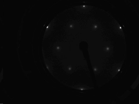
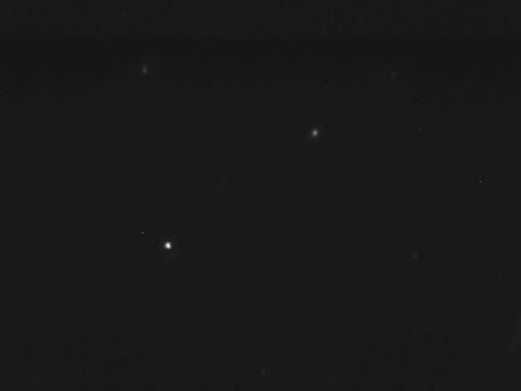
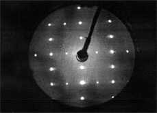
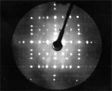
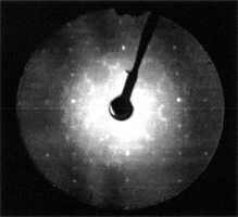
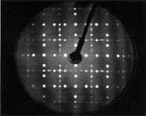
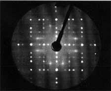
The low energy electron diffraction technique operates by sending a beam of electrons from an electron gun to the surface of the sample being tested. Click here to view an animation illustrating the LEED technique. An electron gun consists of a heated cathode and a set of focusing lenses which sends the electrons between 20-300keV. As the electrons collide with the surface of the sample, they diffract in numerous directions depending on the surface crystallography. Once the electrons diffract, they head back towards three girds followed by a phosphor covered screen. The first grid is grounded and basically serves as a shield which protects the second grid as a result of its negative potential. The second grid acts as filter by allowing only the electrons with higher energies to pass through. The lower energy electrons are blocked out due to the fact that they disorder the image creating a clouded image. Once the electrons pass through the second grid, they come to third and final grid. This grid separates the pervious negative grid from the phosphor screen which carries a positive charge. As the electrons land on the phosphor screen they create a phosphor glow. The intensity of the glow depends on the intensity of the electron. The pattern of these glows is the pattern of the atoms on the surface of the crystal structure. These are the images produced by LEED. Click here to view a few examples of these images.
The general method for analyzing these diffraction patterns was to manually take several dozen pictures. However when computers became available, these photographs were scanned and digitized and the computer ran a program to do the analysis thus saving some time on the experimentalist's part. Later a design was constructed such that the electrons were diffracted directly into a special camera and computer with an imaging software which immediately digitized and analyzed the pattern.
Source: Surface Analysis Methods in Material Science 2nd Edition
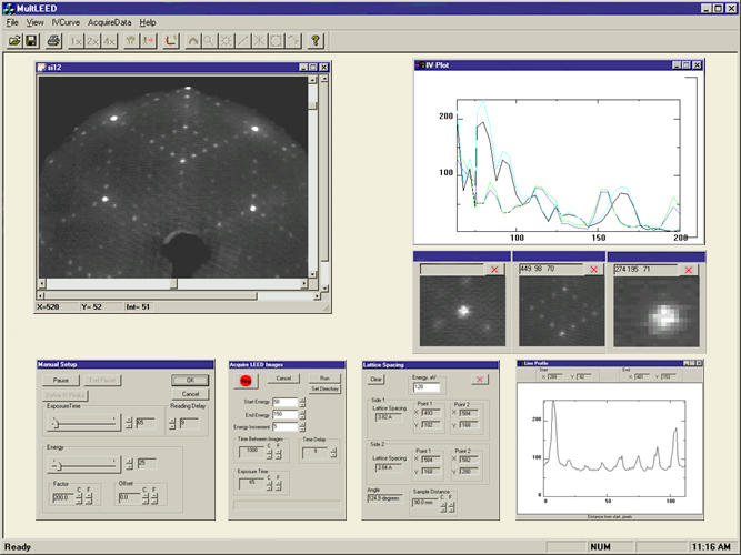
OCI Vacuum Microengineering Inc. offers LEED Image Analysis System that contains low light integration CCD camera, frame grabber, [imaging and analysis software] and ambient light cover.
Find out more on the LEED Image Analysis System product page